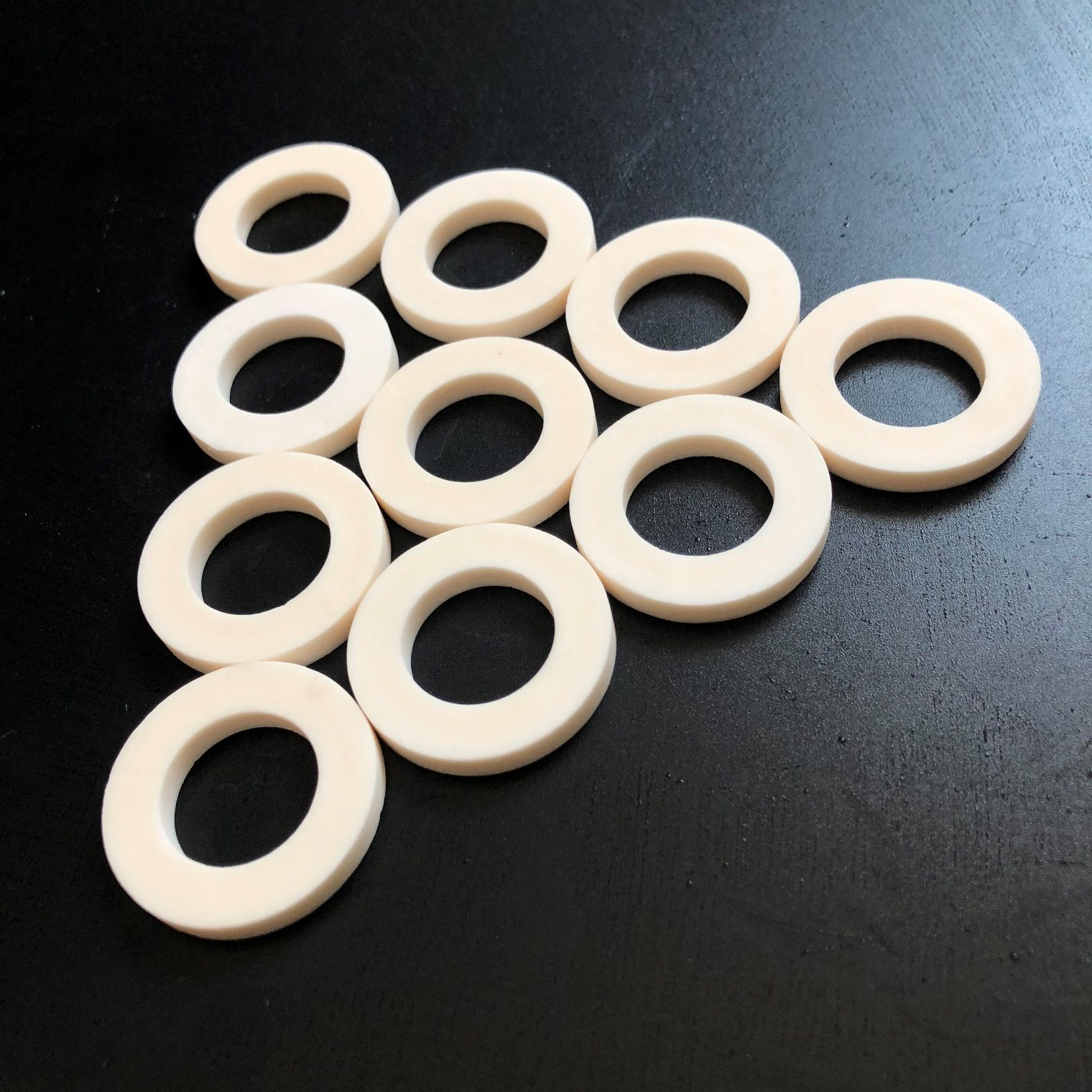
High purity alumina ceramic lined protective wafer

In the etching process of a semiconductor manufacturing enterprise, the plasma etching process produces highly corrosive substances, which can easily contaminate the wafer and seriously affect the performance and yield of the chip. To solve this problem, the company has customized high-purity alumina ceramic lining. The lining is made of 99.3% high-purity alumina ceramic, which effectively resists chemical erosion during plasma etching due to its excellent corrosion resistance. After using this customized liner, the wafer contamination rate has significantly decreased and the chip yield rate has significantly improved. Not only does it reduce production losses caused by pollution, but it also enhances the market competitiveness of products, bringing considerable economic benefits to enterprises. Meanwhile, due to the high hardness and wear resistance of alumina ceramics, the service life of the lining is significantly extended, reducing equipment maintenance costs and downtime, further improving production efficiency.
In physical vapor deposition (PVD) and chemical vapor deposition (CVD) processes, there are extremely high requirements for wafer loading and temperature control. Semiconductor equipment manufacturers have customized aluminua ceramic electrostatic chucks for customers to meet this demand. This electrostatic chuck is made of high-purity alumina ceramics with a purity of over 99.3%, and has excellent heat resistance and stability. During the deposition process, the position and temperature of the wafer can be precisely controlled to ensure the uniformity and quality of the film formation. With its high electrical resistivity and good electrical insulation performance, it effectively avoids the damage of static electricity to the wafer, and improves the stability and reliability of the process.
Wafers require frequent handling during the semiconductor manufacturing process, which places extremely high demands on the handling equipment. After adopting alumina ceramic handling arms, a semiconductor company effectively solved the pollution problem during wafer handling. The handling arm is made of high-purity alumina ceramic, which has the characteristics of high temperature resistance, wear resistance, and high hardness. The surface is smooth and not easily contaminated by particles. In a vacuum environment, the handling arm can stably and accurately handle wafers, avoiding product defects caused by contamination. At the same time, its longer service life also reduces the cost of equipment replacement for enterprises, and improves the continuity and stability of production.

