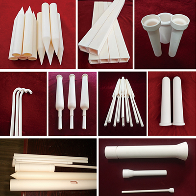
In an era where semiconductor technology is moving towards processes below 3nm, alumina ceramics (Al₂O₃ ceramics) have emerged as a key material supporting the precise operation of semiconductor equipment, thanks to their high purity, excellent insulation, high-temperature resistance, and chemical stability. From chip manufacturing to packaging and testing, alumina ceramics, as the "invisible cornerstone", are driving the continuous innovation of the semiconductor industry.
1. The Core Applications of Alumina Ceramics in Semiconductor Manufacturing
⑴ Key Components of Chip Manufacturing Equipment
Etching and Deposition Equipment: In plasma etching and thin-film deposition (CVD/PVD) processes, alumina ceramics are used to manufacture electrostatic chucks (ESC), gas distribution plates, and chamber linings. Their resistance to plasma corrosion (e.g., against Cl₂, CF₄) and ultra-high flatness (surface roughness Ra ≤ 0.01μm) ensure the precision and stability of wafer processing.
Lithography Technology:Alumina ceramics are used in the mask support structure of extreme ultraviolet (EUV) lithography machines. Its low coefficient of thermal expansion (8.2×10⁻⁶/℃) reduces thermal drift, ensuring nanometer-level lithography precision.
⑵ Packaging and Testing Processes
Integrated Circuit Packaging Substrates: Multi-layer alumina ceramic substrates are used in power modules such as IGBTs and MOSFETs, combining insulation (volume resistivity 10¹⁴ Ω·cm) and heat dissipation functions (thermal conductivity 25W/(m·K)). Their thermal expansion coefficient matches that of silicon chips, reducing thermal stress.
Chemical Mechanical Polishing (CMP): The surface roughness of alumina ceramic polishing plates can be controlled within 0.5 nm, significantly improving the planarization uniformity of wafers and reducing "dishing" defects.
2. Technical Breakthroughs: From Material Modification to Process Innovation
⑴ High Purity and Nanostructuring
The team from the Shanghai Institute of Microsystem and Information Technology, Chinese Academy of Sciences, has recently developed single-crystal alumina gate dielectric materials. These materials can effectively prevent current leakage even at a thickness of only 1 nanometer, providing a new solution for low-power chips. Additionally, nano-alumina ceramics (grain size <200nm), prepared via the sol-gel method, exhibit a flexural strength of 350 MPa—50% higher than traditional materials.
⑵ Composite and Functional Design
Plasma Corrosion Resistance: Yttria-alumina composite ceramics, doped with high-entropy rare earth elements, extend the service life of etching equipment components by more than 10 times.
Intelligent Integration: For example, Jifeng Technology has introduced graphene into alumina ceramics, increasing the thermal conductivity to 200 W/(m·K), making it suitable for heat dissipation modules in 5G base stations.
3. Market Prospect and Localization Process
⑴ Global Market Growth
In 2023, the global market size of alumina ceramic components for semiconductors reached 7.2 billion US dollars, accounting for 45% of precision ceramic components. Driven by demands from AI, 5G, and other fields, the market size is expected to exceed 10 billion RMB by 2025, with China's market share projected to rise from 30% to 35%.
⑵ Localization Breakthroughs
China's self-sufficiency rate of high-purity alumina ceramics (purity ≥99.9%) has exceeded 80%. Enterprises such as Yunxing industrial ceramic are expanding production capacity, planning an annual output of 300 tons of high-purity powder. At the policy level, the New Materials Industry Development Guide has listed high-performance alumina ceramics as a key research direction, aiming to achieve a localization rate of over 85% for key equipment by 2026.
4. Future Trends: Green Manufacturing and Emerging Scenarios
Low-Carbon Processes: Low-temperature co-firing (LTCC) technology reduces energy consumption by 25%, while microwave sintering cuts carbon emissions by 30%.
Emerging Applications: Huge potential exists in scenarios such as hydrogen fuel cell seals, 3D-printed ceramic parts (with a precision of 0.1 mm), and heterojunction photovoltaic cell carrier plates.


